Printed circuit boards: A mobile market
Glass fiber/epoxy prepregs have dominated the mammoth PCB market for decades. Will that continue in a time of great change?
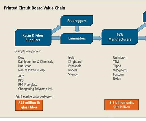
Glass fiber/epoxy laminates have been the foundational structural substrate in printed circuit boards (PCBs) for decades. These iconic thin, green “cards” support the transistors, resistors and integrated circuits at the heart of almost all digital technologies and connect them electrically via conductive pathways etched or printed on their surfaces. They are the world’s largest market for glass fiber, says Drew Walker, CEO of specialty glass fiber producer AGY Holding Corp. (Aiken, S.C.). Indeed, market research firm Lucintel (Irving, Texas) reports a global market for glass fiber in PCBs of 844 million lb in 2013 and forecasts a compound annual growth rate (CAGR) of 4.5 percent. At that rate, the use of glass fiber in the PCB market will reach 1.1 billion lb by 2019. The growth will be fueled by the proliferation of mobile devices and digital control in appliances and cars, and new robotic applications in medical, defense and other manufacturing industries.
Glass/epoxy’s dominance, however, is under challenge as a variety of trends — notably, toward miniaturization, better thermal management, increased speed and performance, and the 3-D printing process — force PCB manufacturers to re-examine their material options. Will glass fiber composites meet tougher specifications as electronics development careens into unknown territory?
FR-4 as industry standard
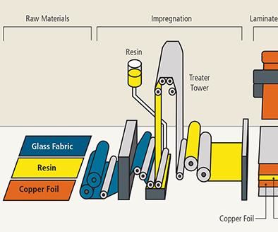
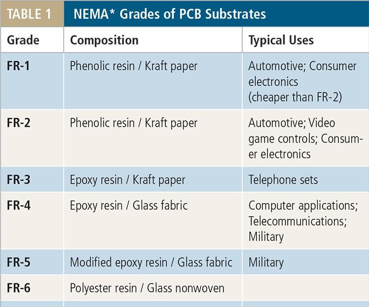
An understanding of the impact of current trends on composites begins with the PCB material and its manufacture. A PCB substrate can be made from paper, glass fiber in woven or nonwoven form, or a composite of paper and glass fiber (hence the term Composite Epoxy Material, or CEM grade, see Table 1, at left). Paper is easier to punch, but fiber provides more strength and stiffness. These materials can be impregnated with a variety of resins, but epoxy is the most common. Higher performance PCBs might also use metals or ceramics as a substrate. FR-4 (Fig. 1, at left), which uses only woven fiberglass and epoxy, has become the standard substrate for PCBs. It functions well as an electrical insulator, is both manufacturable and versatile, and it provides good strength-to-weight at reasonable cost. FR-4’s flame resistance is a plus because electronic devices typically contain their own power sources.
Laminate supplier Norplex-Micarta (Postville, Iowa) describes the significant and increasing requirements FR-4 must meet: Dimensional stability, high mechanical strength, machinability and static dissipation are primary requirements. PCBs are routinely exposed to excessively high temperatures, not just during manufacturing operations, such as soldering, but also in service. Norplex explains that FR-4 materials must function in continuous temperatures of 210°C/410°F while exhibiting very little creep, warp or flex, and also must withstand dramatic temperature fluctuations while resisting moisture absorption. Further, as electronic devices get smaller, assemblies get denser and consistency is even more critical. And the greater number of holes drilled in today’s smaller PCBs — the distance between adjacent holes can be as little as 0.03 inch/0.76 mm — can compromise substrate rigidity.
A PCB substrate must have good dielectric performance. That is, it must insulate the conductive layers from one another by blocking electrical conductivity, to minimize electrical signal loss, crosstalk between conductive layers and noise. Technically, that translates into a low dielectric constant (Dk ≤3.7) and a low dissipation factor (Df ≤0.005). The higher the Dk, the lower the speed of the electrical signal. Df is a measure of the loss in dielectric property, in this case, the insulative capability of the PCB’s composite substrate. Because signal loss and noise are exacerbated by heat, substrates must contribute to thermal management as well.
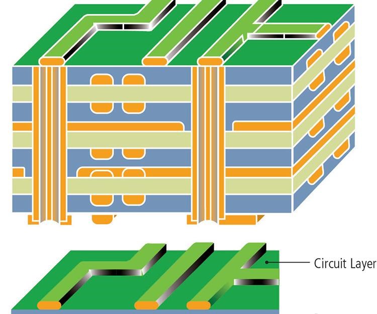
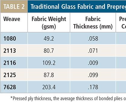
Materials also must be amenable to laminate and circuit-board manufacturing processes. Multiple layers of prepreg are clad with thin copper foil to become a laminate (also called copper-clad laminate, CCL) or a core. Subsequent operations transform laminates into printed circuit boards. PCBs can be classed as rigid, rigid-flexible or flexible: Rigid boards have three basic forms. A single-sided PCB, which has copper on one side, a double-sided board, which uses copper on both outer skins, and multilayer PCBs, which have two or more interleaved layers of copper and glass fiber prepreg connected by “vias” or pathways that are drilled and plated during fabrication (see “Update: Composite PCBs,” under "Editor's Picks). Multilayer PCBs (Figs. 2 and 4, at left) feature single- or double-sided boards as cores with high resin content (HRC) glass fiber prepregs in between to isolate the circuit layers in the stack, which is consolidated in a heated press. This is important because when the electrical signal passes over a fiber, the Dk is higher. The result is greater impedance. That is, the signal is impeded: it actually slows the signal. So the greater the resin-to-fiber content of the layer, the less the prepreg slows the signal. Resins have lower Dk (lower impedance) so the signal speed is higher. Therefore, where FR-4 laminates typically average 50 percent resin by weight, HRC versions might reach 60 to 70 percent resin content. Table 2 (below) shows common prepregs used in multilayer PCBs. Rigid PCBs are distinct from rigid-flexible PCBs, which use unreinforced polymer layers between rigid cores, and flexible PCBs, which use only unreinforced polymer (no composite content).
The market and value chain
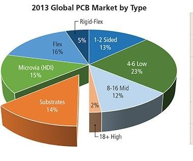
According to industry sources, the global PCB market has grown from $35 billion in 2006 to a 2013 value of $62 billion (see Fig. 3), but the U.S. share has dropped from 15 percent to 5 percent, with 90 percent of PCBs now manufactured in Asia. North America still maintains a number of important technology players, including laminate producers Isola and Rogers Corp. (both in Chandler, Ariz.) and PCB producer TTM Technologies Inc. (Costa Mesa, Calif.) as well as a host of small prototyping and specialty manufacturers.
According to TTM Technologies, multilayer PCBs (including 4 to 6 layers, 8 to 16 layers and 18+ layers, see below) make up 47 percent of the market, with the highest growth projected for 8- to 16-layer boards. Rigid-flexible PCBs, now only 5 percent of the market, are forecast to grow fastest, reflecting the move toward smaller, higher-performance electronic devices. This trend also pushes growth projections for high-density interconnect (HDI) and flexible PCBs, the latter used in liquid crystal displays (LCDs) and touch screens. China’s 11th Five-Year Plan confirms this market picture, listing multilayer, flexible, flexible-rigid and environment-friendly (see “PCB environmental concern: Hit and miss,” under "Editor's Picks") PCB technologies as keys to China’s electronics and information technology sectors during the next 5 to 15 years.
Lucintel predicts that E-glass and epoxy resin will remain dominant in PCB manufacturing in the near term and notes that glass fiber manufacturers are decreasing yarn diameters to meet the market need for miniaturized devices. Common yarns, comprising 200 or 400 filaments in a 7- or 9-micron diameter, will give way to 50-filament, 4-micron yarn. AGY introduced two new yarns of this description in 2013. Its 4-micron yarn line, started in 2010, now numbers four distinct products.
Another emerging trend is the development of low-loss glass fiber to meet HDI board requirements. Lucintel cautions that PCBs are facing many challenges, among them, thermal fatigue and coefficient of thermal expansion (CTE) mismatch. Consequently, glass fiber could come under attack as R&D programs seek materials that can provide the higher performance now demanded in almost all market segments.
Less room, more heat
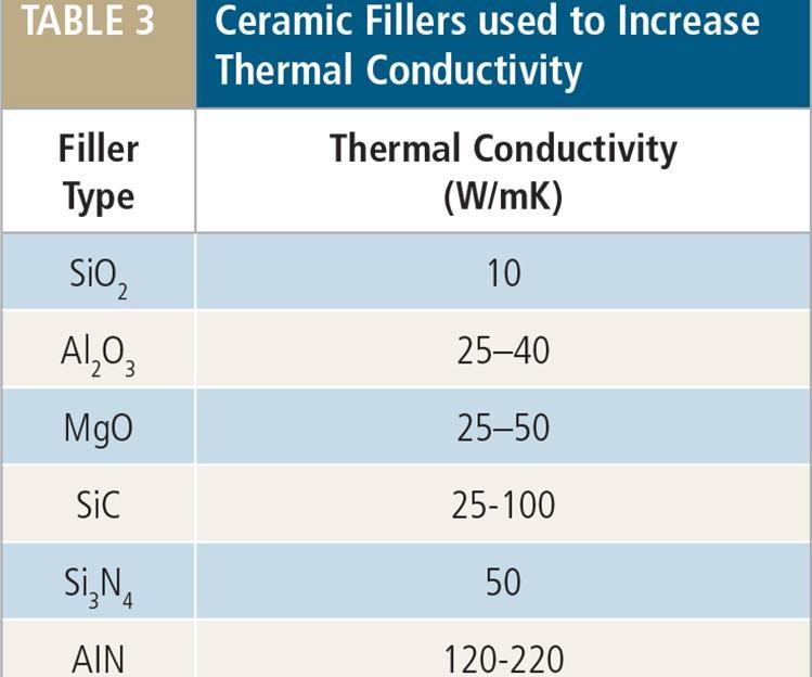
As computers and mobile devices get smaller, faster and more sophisticated, more heat-producing internal electronics are packed into smaller spaces, increasing temperatures in PCB laminates and, thus, threatening performance. Elevated temperatures in cell phones, for example, push chemical reactions in the lithium-ion batteries, necessitating more frequent recharging. The increased use of light-emitting diodes (LEDs) — e.g., keypads, cell phone camera flashes and backlight units (BLUs) for screens — is driving the use of insulated metal cores (IMCs) or metal core PCBs (MCPCBs). For these applications, aluminum is most commonly used, followed by steel and copper. The thermal conductivity of a standard FR-4 laminate is only 0.25 W/mK. Standard IMC substrates boast up to 8 W/mK, and R&D units are aiming higher. Polymer (typically epoxy) with or without glass fiber remains the common insulation (dielectric) layer between the copper circuit and metal substrate. However, because glass is a good thermal insulator, thermally conductive ceramic fillers (see Table 3) have been added to the prepreg resins, increasing their heat transfer by a factor of 12 and enabling their use as a bonding layer for the heat-dissipating metal base. Still, unreinforced polymer layers using these same fillers have increased heat transfer more than 25 times, with development continuing.
Composites may find an opportunity as traditional cooling methods come up short. Passive techniques include adding heat spreader layers (e.g., high-thermal-conductivity copper) that are connected directly to heat sources by multiple vias. Active techniques include fans. These are no longer enough. One solution is to integrate other traditional methods, such as heat pipes (a micro air conditioner, using fluid and condenser), fin heat exchangers and piezoelectric fans, into the PCB laminate, saving space and improving thermal conductivity. The University of California Los Angeles (UCLA, Los Angeles, Calif.) published the results from integrating a heat pipe directly into an FR-4 PCB and measured a thermal resistance less than one-sixth that of an FR-4 and one-half that of a metal-cored PCB.
The ability to fabricate composites on an ever-smaller scale also might offer heat and performance solutions. For example, a team from Stanford University (Palo Alto, Calif.) recently demonstrated a computer that uses transistors made from carbon nanotubes (CNTs) rather than silicon. As silicon transistors shrink in size — billions of these tiny on-off switches are now integrated into computer chips — they become less efficient, wasting power and generating heat. CNTs are exceedingly thin — thousands could fit in a human hair — so it takes very little energy to switch them off. They are also very efficient electrical conductors. Thus, electronics made using CNT transistors could be smaller, run faster and use less energy than those made with silicon chips. The use of CNT/epoxy in PCB laminates and within vias to increase conductivity also is being explored. Like structural health monitoring networks in composite aircraft wings or turbine blades, CNTs might offer potential for embedded networks within PCBs that achieve greater electrical conductivity with less heat.
Mitigating CTE mismatches
As devices get more compact, there is less room to accommodate a material’s expansion or contraction as internal temperature fluctuates. PCB manufacturer Elmatica (Oslo, Norway) lists the coefficient of thermal expansion (CTE) for a typical FR-4 as 14 to 17 ppm/°C. Yet components attached to the PCB can have an expansion rate as low as 6 ppm/°C. This difference is enough to shear solder joints when the PCB heats up.
Another issue for composites, says Tarun Amla, executive VP/CTO for PCB laminate source Isola Group, is that “glass/epoxy composites exhibit anisotropy, both in dielectric constants and dissipation factors. For example, CTE in the x and y directions may range from 12 to 25 x 10-6 m/m, but is closer to 40 to 90 x 10-6 m/m in the z-direction.” He suggests that demand for isotropic substrates might reduce the use of glass/epoxy in PCBs.
Elmatica maintains that using metal cores — e.g., copper-Invar-copper (CIC) and copper-molybdenum-copper (CMC) — is expensive and presents machining issues, as do laminates made with aramid fibers. Elmatica, therefore, favors STABLCOR, a thermally and electrically conductive laminate available in carbon fiber/epoxy or carbon fiber/polyimide. Developed by NASA, the material is supplied to licensed manufacturers only by STABLCOR Technology Inc.(Huntington Beach, Calif.). The company explains that STABLCOR does not replace all FR-4 laminates in a multilayer PCB, but instead is used selectively to reduce CTE mismatch and improve thermal management. Integration of STABLCOR at the right location in the PCB stack reportedly makes a CTE of 8 to 10 ppm/°C possible and increases rigidity without adding weight. Many other materials are being explored to help produce lower CTE laminates, including liquid crystal polymers and ceramic matrix composites (CMCs).
Abating pad cratering
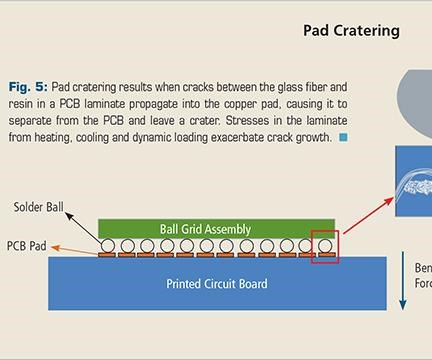
There also can be a mismatch between a PCB substrate’s CTE and the temperatures and dynamic loads it sees in service. This can lead to pad cratering, where cracks — which form between the glass fiber and resin in the PCB laminate — propagate into the copper pad, causing it to separate from the PCB and leave a crater. As the industry has moved to more environmentally friendly lead-free solder and high-density, enabling ball grid arrays (BGAs), pad cratering has become an electronics failure issue. BGAs use rows of solder balls on the PCB to conduct electrical signals (Fig. 5). Lead-free solders are more brittle than lead/tin predecessors, and soldering requires more time at higher temperatures. Because FR-4 degrades at these higher temperatures, phenolic grades were developed. Unfortunately, these also tend to be brittle.
Jim Griffin, OEM marketing manager for Integral Technology (Lake Forest, Calif.), explains that the solder balls at the BGA edges cool and solidify faster than those in the center, while PCB laminates can twist slightly with heat and then flatten as they cool. Stresses introduced by these phenomena can leave the substrate less resistant to fracture if the device is dropped or flexed. That fracture grows as the heat generated in the device causes further expansion and contraction. Griffin summarizes, “Pad cratering is the result of the technology exceeding the capabilities of the materials.”
Integral Technology claims to have the only pad cratering solution in Zeta Cap, a high-temperature, unreinforced polyimide film. Designed as an extra layer between the outermost copper foil and dielectric layer, Zeta Cap’s high mechanical strength prevents the pad from peeling away. Its lack of fiber reportedly improves board flexibility, which, according to Griffin, “results in less stress on both the PCB laminate and lead-free solder joints.”
Although polyimide offers high resistance to pad cratering, it is also more expensive and more difficult to process than epoxy. Research by others into pad-cratering-resistant materials, so far, shows little progress with epoxy-based laminates. However, Ryerson University (Toronto, Ontario, Canada) has demonstrated that reducing a resin’s hardness correlates strongly to increased pad crater resistance in the laminate.
Taking a completely different approach, Laser Zentrum Hannover eV (LZH, Hannover, Germany) and partners are developing a multilayer PCB, using thin (145-µm thick) glass sheets as a base. They believe that the material’s high chemical stability and low CTE will help fabricators achieve miniaturization and higher processing speeds in PCBs for high-temperature applications (>250°C/>482°F). Thin glass plate is also completely recyclable and can be made from recycled content. A laser makes conducting traces by removing excess metal from the glass base, reportedly enabling extremely fine structural resolution. Manufacturing feasibility is not yet proven, however. The current focus is on finding laser parameters that will enable drilling through the materials without thermal damage.
CAF mitigation
Another issue threatening glass fiber/epoxy’s reign is conductive anodic filamentation (CAF), the result when copper corrosion residue grows along the glass fiber/resin interface in a PCB laminate as current passes from anode to cathode. CAF can cause fiber/resin separation and can be a significant and potentially dangerous source of electrical failures. One of the selling points for Integral Technology’s unreinforced Zeta Cap is that it also prevents CAF because it lacks the enabling fiber/resin interface.
Isola has developed a patented CAF mitigation technology, available for license worldwide to laminate and prepreg manufacturers and users. The company explains that voids in prepregs are a source of CAF. According to its patent, Isola’s technology enables a laminate that is substantially void-free by removing moisture from the substrate prior to impregnation and then using discrete zones, first of low solids and then high solids resins, as well as explicit heating through the process.
Other CAF prevention measures include, for example, the use of spread-tow fabrics in PCB laminates. Because these are thinner and each is only one-fiber thick, they enable better wetting of the fibers during application of the coupling agent than can be done with conventional, tightly bound glass fiber bundles. This reduces the risk of resin/fiber separation.
Priority on performance
Flatter fabrics also improve signal speeds across PCB laminates, notable because delivering desired transmission rates is a must if FR-4s are to endure. The effect of fabric weave can be seen in a conventional 106-style glass cloth, because fiber gaps, which make up 40 percent of the volume, are filled with resin. Art Aguayo, senior business development manager at Rogers Corp., explains, “In high-frequency applications, the signal wavelength is so small [≈3 mm] that the weave pattern of the glass fabric interrupts it.” In other words, as noted previously, signal speed through copper traces placed directly over high-fiber content substrates tend to impede the signal more than substrates that are resin-rich. Therefore, if two signals are headed for the same destination via two copper traces, and one passes over a fiber-rich substrate while the other passes over a resin-rich substrate, they will arrive out of sync. Technically, they are out of phase, that is, at the precise point in time at which they arrive, the two signals are at different points in their wave cycle. Signals that are 180° out of phase — one signal is at the top of its wave cycle when the other is at the bottom, will actually cancel each other out. So the more out of phase the signals are (signal skew), the greater the signal loss and the greater, therefore, is the Df of the substrate. Isola’s Amla notes, “Skew is the biggest barrier to reaching speeds beyond 28 GBps per channel over longer distances.”
One way to mitigate these micro-Dk effects is to minimize the gaps between yarns, creating a more homogeneous substrate. Conventional glass cloth styles have been replaced by more “square weave” alternatives, which add yarns so that warp and weft directions have nearly the same thread count. Another tack is Isola’s newly developed GigaSync material. The company claims it enables low loss, low skew and high speed by matching the dielectric constant in the glass weave to that of the resin. According to Alun Morgan, director of OEM marketing for Isola Europe, “This applies to all combinations of glass styles used in a stack-up because the resin content no longer has an influence on the dielectric constant, thus simplifying the electrical design.”
Demand for higher performance is driving not only reduced Dk, reportedly possible with low-Dk glass fiber, but also lower loss factor (Df). However, reducing both simultaneously is especially challenging. Rogers Corp. uses polytetrafluoroethylene (PTFE, i.e., Teflon) and higher performance thermoset resins with glass to reduce electrical loss, says Aguayo: “And now we are using unreinforced resins — basically flexible circuit board materials — replacing the glass weave with ceramic particles.” He notes that this is still a specialty market — accounting for 5 percent of PCBs, in terms of dollar value — because mass-market FR-4 laminates cost ~$2.00/ft2 while high-end PTFE-based materials range from $8/ft2 up to $100/ft2. The result is a Catch-22 of sorts, notes Aguayo: “The price won’t come down until high-volume production is committed, but most manufacturers can’t commit to high volume without a price drop.” That said, top-20 PCB manufacturer Gold Coast Electronics (Chung-li, Taiwan) predicts a 50 percent cost drop in the next few years as “getting by” with mid-loss materials succumbs to performance pressure, and low-loss materials enter the mainstream. Aguayo, however, thinks this is still years away.
Perhaps the ultimate low-loss, high-speed solution is optical boards, or rather the integration of optical transmission paths into the PCB, creating a hybrid electrical-optical PCB (EOPCB). Although the more common approach is to embed unreinforced polymer between FR-4 layers as waveguides for optical signal transmission with interconnected fiber cables, Fraunhofer Institute for Chemical Technology (ICT) (Berlin, Germany) is integrating the optical waveguides into thin glass sheets. Aguayo says the optical-board option also was forecast to transform the PCB market, “but it has remained a niche, while the industry has found other ways to jump in speed and performance with the materials it has.”
Nanotechnology and 3-D printed circuits
“Although the composites industry is working towards novel solutions to structural problems such as self-healing composites,” observes Amla, “we have not seen much movement toward PCB-related problems.” Isola, however, is looking at nanofillers. Amla explains, “Engineered isotropic standalone films with elastic modulus exceeding 15 GPa could act as substrates for printed circuit boards and also be designed to substantially reduce the risk of pad cratering and CAF.” The company is already working to improve thermal, mechanical and electrical properties through the use of nanotechnology. “Isola is using computational tools for modeling from quantum scale to board level in order to build optimal properties in the composite and the polymer,” Amla explains. “We are pursuing engineered isotropic dielectrics, whether in film or composite form.”
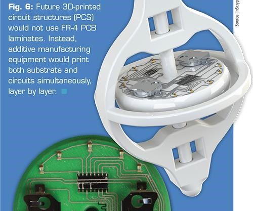
Yet, many experts agree that the next logical step in the continuing push for performance is to move beyond stacked laminates into 3-D printed structures. According to an article from nScrypt Inc. (Orlando, Fla.) in the July 2013 issue of The PCB Magazine, the solution is to “eliminate the traditional 2-D FR-4 board and the wires, epoxies, vias and solder and make the next-generation packages utilizing 3-D: the printed circuit structure (PCS).”
It is now possible to combine one of the variety of proven 3-D printing techniques with an established commercial printed electronics process and successfully build complete electronic products that exhibit the small feature sizes, high density and high performance now in demand. Traces, resistors, antennae and other subcomponents can now be printed “up, around and within.” Possible advantages include hiding components within structure to hinder reverse engineering and prevent fluid entry, increasing ruggedness by eliminating glue, solder and wiring, and achieving the ultimate in volumetric optimization by enabling many more functions in smaller spaces. PCS demonstrations from the early 2000s have progressed toward commercially viable alternatives to traditional manufacturing, and because the printed structure is the circuit carrier, there is no need for PCBs (Fig. 6).
Currently, 3-D printing and digital electronics printing are completed in successive operations. As yet, no commercially viable system can fully print both structure and circuits simultaneously. In her 3Dprint.com article “Neotech Announces Release of 3D Printed Electronics Platform,” author Hannah Rose Mendoza asserts, “It is only a matter of time before Neotech [Nuremberg, Germany] or someone else develops an integrated electronics printer capable of producing both the object and its electronics at the same time.” Neotech already has taken many steps toward that goal. It developed the world’s first five-axis 3-D printed electronics system in 2010, using four Aerosel Jet print heads (made by Optomec, Albuquerque, N.M.) that can produce complex circuitry on almost any 3-D surface. Already, Neotech’s machines are making mobile device antennas that, according to Mendoza, do not require “any hard tooling, special plastic resins or plating” thanks to the “digitally driven process.”
Meanwhile, nScrypt Inc. claims its direct printing additive manufacturing (DPAM) system is able to combine 3-D printing’s structures with printed electronics’ functionality. But it is still in early development and, as yet, labor-intensive. The company is researching materials to achieve specific mechanical and electrical properties with 3-D building and process refinement to mitigate surface roughness and voids.
Again, composites’ ability to move progressively down the micro scale will likely enable new materials for these 3-D processes. But, eventually, the market for woven fabrics impregnated with resin will be impacted.
Aguayo, however, says the biggest risk is the move to place more electronics on a single semiconductor chip, called system on a chip. He explains, “You still use a PCB but it is much smaller because all of the components you previously mounted are now integrated onto a small solid-state chip. So you have much less circuit area, requiring much less board material.”
He sees this trend as widespread and consistent with the coming of the “connected car” and increased use of sensors everywhere. “Who knows what materials will be needed for these?” he wonders. “Perhaps the sensors will need to be oddly shaped and flexible or very small.”
Aguayo concludes that change is inevitable, but he points out that “FR-4 is like the combustion engine. Are there new developments coming that could replace it?” he asks. “Yes. But it’s still going to be around for quite a while.”
Related Content
The potential for thermoplastic composite nacelles
Collins Aerospace draws on global team, decades of experience to demonstrate large, curved AFP and welded structures for the next generation of aircraft.
Read MorePlant tour: Teijin Carbon America Inc., Greenwood, S.C., U.S.
In 2018, Teijin broke ground on a facility that is reportedly the largest capacity carbon fiber line currently in existence. The line has been fully functional for nearly two years and has plenty of room for expansion.
Read MorePEEK vs. PEKK vs. PAEK and continuous compression molding
Suppliers of thermoplastics and carbon fiber chime in regarding PEEK vs. PEKK, and now PAEK, as well as in-situ consolidation — the supply chain for thermoplastic tape composites continues to evolve.
Read MoreCryo-compressed hydrogen, the best solution for storage and refueling stations?
Cryomotive’s CRYOGAS solution claims the highest storage density, lowest refueling cost and widest operating range without H2 losses while using one-fifth the carbon fiber required in compressed gas tanks.
Read MoreRead Next
Update: Composite PCBs
Small printed circuit boards are big consumers of composite materials.
Read MoreDeveloping bonded composite repair for ships, offshore units
Bureau Veritas and industry partners issue guidelines and pave the way for certification via StrengthBond Offshore project.
Read More

