Metal Matrix Composites Advance Optoelectronics Package Design
Cast aluminum silicon carbide keeps costs down while providing ideal thermal properties.
The science of optics plays a crucial role in modern society. Televisions, CD and DVD players and recorders, bar code scanners, digital cameras, laser printers and fiber optic communications equipment rely on light for the transmission of data. However, data cannot be handled solely as light, so special optoelectronic devices convert between optical and electrical signals.
An optoelectronic device comprises several components, and might include lasers, laser diodes, optical fibers, lenses, mirrors, semiconductor devices, copper lead wires and other items. These individual components are assembled into a package to form the optoelectronic device. The package may be made from special metal alloys, polymer matrix composites or metal matrix composites.
A number of factors influence packaging materials selection, including raw material cost, manufacturing processes, dimensional tolerances and material properties (density, strength, stiffness, electrical resistance and others). Thermal properties, however, are by far the most important. An optoelectronic device is assembled from several different components, each of which can be made of a different material. The components are assembled using a variety of methods, including brazing, soldering, welding and adhesive bonding. Since all of these materials can have different coefficients of thermal expansion (CTEs), elevated assembly temperatures can create permanent mechanical stresses that can affect alignment tolerances or damage components.
In use, electronic components generate heat, which means that optoelectronic devices must withstand thermal cycling (on/off) or a constant elevated temperature. In-service temperature changes can lead to additional thermally induced stresses. Furthermore, packaging must be designed to dissipate heat in order to keep the temperature at a reasonable level and avoid damaging sensitive components.
AlSiC as a packaging material
The telecom boom of the 1990s created an enormous demand for optoelectronic devices, fueled in large part by an expected explosion in Internet traffic. According to Dave Saums, vice president of marketing for Ceramics Process Systems Corp. (CPS, Chartley, Mass., U.S.A.), manufacturers took a "brute-force" approach to package design to keep up with demand. Packages were often built as copper-tungsten (Cu-W) "bathtubs" machined out of solid bar stock. The Cu-W packages are simple and quick to design, and provide good thermal properties, but they also are heavy and require relatively expensive CNC machining.
Since Internet traffic never reached expected levels, Saums estimates that 70 to 80 percent of the installed fiber in North America remains dark (out of service). In the wake of the telecom crash, FibreSystems Magazine reports that excess inventory has forced optoelectronic prices to drop by as much as 40 percent. As market demand returns, price-sensitive end-users will keep a downward force on prices. Manufacturers must find a way to lower costs or see profit margins erode.
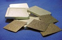
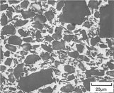
CPS specializes in the manufacture of packaging made from aluminum silicon carbide (AlSiC), a metal matrix composite in which an aluminum matrix impregnates a uniquely processed filler "preform" made from microscopic silicone carbide particles. AlSiC has been used for many years as a package material in general electronics applications, and in more specialized applications such as processor, radio frequency (RF) and microwave components. Recently, there has been increased interest in the use of AlSiC for optoelectronics packaging because of its compatible CTE, high thermal conductivity, and for the potential to produce parts at low cost.
The combination of low material costs and net-shape casting makes AlSiC a cost-effective alternative. The SiC particles typically cost about $8.82/kg ($4.00/lb). The aluminum 356.2 — a common casting alloy — costs about $1.76/kg ($0.80/lb). Modern optoelectronic packages are modular in design, making direct comparisons to monolithic Cu-W "bathtubs" difficult. But an AlSiC lid (a part that provides mechanical protection and heat dissipation to an attached semiconductor), for example, can cost as little as $4. A Cu-W package for a similar application might cost $40-$50. Although the Cu-W package performs multiple functions, an AlSiC package made from several parts still would be much less expensive. More importantly, AlSiC is more versatile than Cu-W, because it can accommodate added features such as embedded materials and active cooling. These extras increase the package price — most often modestly, though large, highly complex components might cost $7,000 or more — but they provide functional sophistication required in today's more complex optoelectronic devices that would be impossible to achieve with Cu-W.
The manufacturing process developed by CPS is somewhat like a cross between injection molding and resin transfer molding (RTM). Mark Occhionero, senior scientist at CPS, describes the process in more detail: To begin, SiC particles are mixed with a proprietary carrier liquid to form a slurry with about 35 to 67 volume percent SiC, depending on the desired thermal properties (as described below). Next, the slurry is injected into a cold steel mold under relatively low pressure (1,379 to 6,895 kPa/200 to 1,000 psi). In about 15 seconds, the slurry freezes into a solid mass that can be handled. The part is moved to a freezer where the carrier liquid sublimates, leaving a porous, SiC preform. Because the carrier goes directly from a solid to a gas, the SiC particles maintain their structure, held together by remaining slurry additives and intermolecular (van der Waals) forces. The composite is formed by placing the preform into a mold and infiltrating molten aluminum under pressure to fill the pores. After demolding, the part is mechanically deflashed, then tumbled or sandblasted (depending on smoothness requirements).
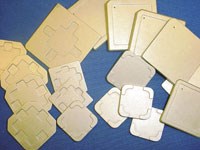
The casting process produces a net-shape part, so in most cases no additional machining is required. In general, the process can hold tolerances to ±0.076 mm/0.003 inch in the plane of the part, ±0.051 mm/0.002 inch through the thickness, and ±0.025 mm/0.001 inch on drilled holes. Minimum thicknesses are 0.813 mm/0.032 inch on walls, 0.51 mm/0.020 inch on the base, and 0.381 mm/0.015 inch on small areas of the base. A minimum 3° draft angle is required on the outside walls to enable removal from the mold; typically 5° is requested to improve the infiltration casting mold life and reduce manufacturing costs.
Thermal properties
By adjusting the volume of SiC particles in the composite, CPS can tailor the CTE to a desired value. CPS offers three standard grades of AlSiC (AlSiC-9, -10 and -12) with CTEs of 8.75, 10.56 and 11.5 ppm/K, respectively. The specific grade is chosen to match other materials in the assembly. For example, AlSiC-9 is a good match for gallium arsenide (GaAs) and silicon (Si), common integrated circuit (IC) materials, with CTEs of 4.2 and 6.5 ppm/K, respectively. AlSiC-12 is a better match for printed circuit board (PCB) materials, with CTEs in the range of 14 to 17 ppm. Because the AlSiC has a slightly higher CTE than the IC materials, the thermal stresses put the ICs into slight compression after bonding, improving crack resistance.
To dissipate excess heat, the package must have a high thermal conductivity. AlSiC-9 and -10 have a thermal conductivity of 180 W/mK (104 Btu/(h·ft·°F)); AlSiC-12 has a thermal conductivity of 170 W/mK (98.2 Btu/(h·ft·°F)). This compares well with 180 W/mK for Cu-W, and 170 W/mK for copper-molybdenum (Cu-Mo). Kovar, another common packaging material, chosen for its low CTE of 5.2 ppm/K, has a thermal conductivity of only 17 W/mK (9.8 Btu/(h·ft·°F)).
When a constant temperature must be maintained in the optoelectronic device, customers often include a thermoelectric cooler in the design. A thermoelectric cooler is basically a semiconductor device that pumps heat from one side of the package to the other when a current is applied (thermoelectric coolers aren't limited to high-tech electronics — they also cool the electric ice chests manufactured by companies like Coleman and Igloo). For the cooler to operate effectively, the package must not only dissipate the heat, but it must maintain a uniform temperature over the hot surface, as well.
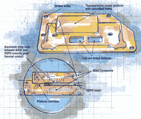
Packaging materials alone, including AlSiC, do not have a high enough thermal conductivity to maintain a uniform temperature, so manufacturers have adopted several methods to boost their conductivity. One approach is to embed cooling pipes into the package, pumping a liquid through the pipes to draw out the heat. Another approach is to embed a layer of material with extremely high thermal conductivity, such as highly oriented pyrolytic graphite (HOPG) or CVD diamond, into the package.
The HOPG or CVD diamond is inserted into the SiC preform prior to the casting of the aluminum alloy. A thin layer of aluminum alloy between the HOPG and AlSiC provides excellent thermal contact. HOPG provides a thermal conductivity of 1,350 W/mK (780 Btu/(h·ft·°F)) inplane, but only 10 to 30 W/mK (5.8 to 17 Btu/(h·ft·°F)) through-thickness. CVD diamond provides 1,000 to 1,500 W/mK (577.8 to 866.7 Btu/(h·ft·°F)) in all directions, but costs about 10 times as much as HOPG. A 25.4-mm/1-inch square, 0.38-mm/0.015-inch thick HOPG insert adds about $3 to $4 to the cost of the AlSiC component.
Future applications
AlSiC's thermal properties have made it an attractive packaging material for electronic and optoelectronic applications. The casting process developed by CPS, which produces net-shape, zero-shrinkage parts, has further shown that AlSiC packages can be produced at prices that are competitive with more traditional packaging materials. Manufacturing rates currently range from a dozen or so parts per year, for highly specialized military applications, to more than 50,000 parts per year for the electronics industry.
Given AlSiC's properties, the material has a wide range of uses. For example, AlSiC has low density compared to traditional metal components — on the order of one-third the density of copper, and one-fifth the density of Cu-W — making it an attractive material for portable electronics, such as laptop computers and space-based applications. Space station power modules are built on CPS AlSiC baseplates that incorporate large amounts of HOPG, and the U.S. Air Force is considering AlSiC components for space-borne weaponry programs. Further, AlSiCs may find their way into military radar systems, as well, where the lower density can provide significant weight savings for the relatively large components.
Related Content
CompPair adds swift prepreg line to HealTech Standard product family
The HealTech Standard product family from CompPair has been expanded with the addition of CS02, a swift prepreg line.
Read MorePEEK vs. PEKK vs. PAEK and continuous compression molding
Suppliers of thermoplastics and carbon fiber chime in regarding PEEK vs. PEKK, and now PAEK, as well as in-situ consolidation — the supply chain for thermoplastic tape composites continues to evolve.
Read MoreComposite resins price change report
CW’s running summary of resin price change announcements from major material suppliers that serve the composites manufacturing industry.
Read MoreSmartValves offer improvements over traditional vacuum bag ports
Developed to resolve tilting and close-off issues, SmartValves eliminate cutting through vacuum bags while offering reduced process time and maintenance.
Read MoreRead Next
All-recycled, needle-punched nonwoven CFRP slashes carbon footprint of Formula 2 seat
Dallara and Tenowo collaborate to produce a race-ready Formula 2 seat using recycled carbon fiber, reducing CO2 emissions by 97.5% compared to virgin materials.
Read MoreDeveloping bonded composite repair for ships, offshore units
Bureau Veritas and industry partners issue guidelines and pave the way for certification via StrengthBond Offshore project.
Read MorePlant tour: Daher Shap’in TechCenter and composites production plant, Saint-Aignan-de-Grandlieu, France
Co-located R&D and production advance OOA thermosets, thermoplastics, welding, recycling and digital technologies for faster processing and certification of lighter, more sustainable composites.
Read More


