Purdue researchers create single-photon method for large-scale laser-based 3D additive nanoprinting
Patent-pending technology produces high-resolution nanostructures faster and less expensively than traditional laser nanoprinting.

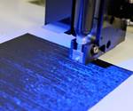
Liang Pan, alongside the team’s 3D printing technology. Source | Purdue University/Jared Pike
Researchers in Purdue University’s College of Engineering (West Lafayette, Ind., U.S.) have developed patent-pending single-photon 3D nanoprinting technology. It is reported to produce a higher throughput of complex, high-resolution nanostructures faster and less expensively than traditional laser-based 3D additive nanoprinting technologies.
According to Liang Pan, professor of mechanical engineering, who is leading the team developing this technology, the printing materials that are being used are similar to the ones incorporated in photocurable resins for other digital light processing (DLP) 3D printers (which can use fiber fillers), though the team has modified some of the material’s composition to improve nanoscale resolution.
The research, says Pan, enables 3D nanoprinting at lower laser intensities without the need for femtosecond lasers. It does not rely on single-point scanning processes and therefore produces high-speed and high-resolution results.
“The technology uses less expensive light sources as simple as a laser pointer, which can reduce the tool cost by 10 to 100 times,” he explains. “The writing speed is a few orders of magnitude faster for each beam, and we can further expand to parallel scan with tens to hundreds of beams.” The single-photon technology has applications in nanotechnology research and industry, manufacturing processes, and health care.
Femtosecond laser two-photon polymerization is widely used for 3D nanostructure fabrication. “However, this technique is expensive and slow, which presents significant obstacles for commercial use in manufacturing,” Pan emphasizes. Alternative options have been developed to increase speed and reduce cost, but they are said to deliver limited resolution and require high-power lasers, unlike Pan’s innovation.
Pan’s single photon-based method uses fast panel writing to construct high-volume and complex nanostructures for wide ranges of use. Notable applications include nanolithography, zero-stiffness microstructures and thermal interface structures.
“We have demonstrated the method by printing 120-nanometer-resolution structures using a low-cost diode laser,” Pan says. “We also demonstrated parallel nanoprinting using a 9 × 9 array laser beam.”
The next steps to develop the technology are further increasing the scanning throughput and reducing the tool cost. Pan and his team are applying for federal funds for research and development.
The National Science Foundation awarded Pan two grants to conduct his research.
Industry partners interested in developing or commercializing it should contact Parag Vasekar, business development and licensing manager, at psvasekar@prf.org, about track code 69873.
Related Content
-
Plant tour: Albany Engineered Composites, Rochester, N.H., U.S.
Efficient, high-quality, well-controlled composites manufacturing at volume is the mantra for this 3D weaving specialist.
-
The potential for thermoplastic composite nacelles
Collins Aerospace draws on global team, decades of experience to demonstrate large, curved AFP and welded structures for the next generation of aircraft.
-
Jeep all-composite roof receivers achieve steel performance at low mass
Ultrashort carbon fiber/PPA replaces steel on rooftop brackets to hold Jeep soft tops, hardtops.


.jpg;maxWidth=300;quality=90)


